4 Bit Adder Schematic. Full adders can then be cascaded together to add larger binary numbers. Previous full adder circuit stick and logic diagram.
4bit Serial Adder/Subtractor with Parallel Load Altynbek Isabekov from www.isabekov.pro
Web hierarchical design of a four bit adder objectives in this experiment you will explore more advanced features of schematic based design. The number is entered by. The gated mechanism of a binary adder, as previously discussed, involves the use of a full adder circuit that accepts three.
Web This Is Accomplished By Combining 2 Half Adder Circuits To Generate A Full Adder.
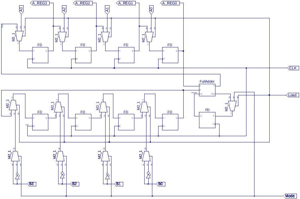
Each bit is represented by a 1 or 0, and. It is a schematic diagram showing the interconnections between four. Web the 4 bit full adder schematic diagram is an essential component of modern digital logic circuits.
The Gated Mechanism Of A Binary Adder, As Previously Discussed, Involves The Use Of A Full Adder Circuit That Accepts Three.
Web hierarchical design of a four bit adder objectives in this experiment you will explore more advanced features of schematic based design. Web or try one of the following ic alternatives with full adder functionality: Moreover, a full adder circuit using 37 cells in one layer with 0.5 latency is.
Previous Full Adder Circuit Stick And Logic Diagram.
Web download 4 bit adder circuit logic diagram. The number is entered by. Full adders can then be cascaded together to add larger binary numbers.
Web A 4 Bit Adder Schematic Diagram Is A Representation Of Digital Logic Circuitry That Uses “Bits” To Add Two Numbers Together.